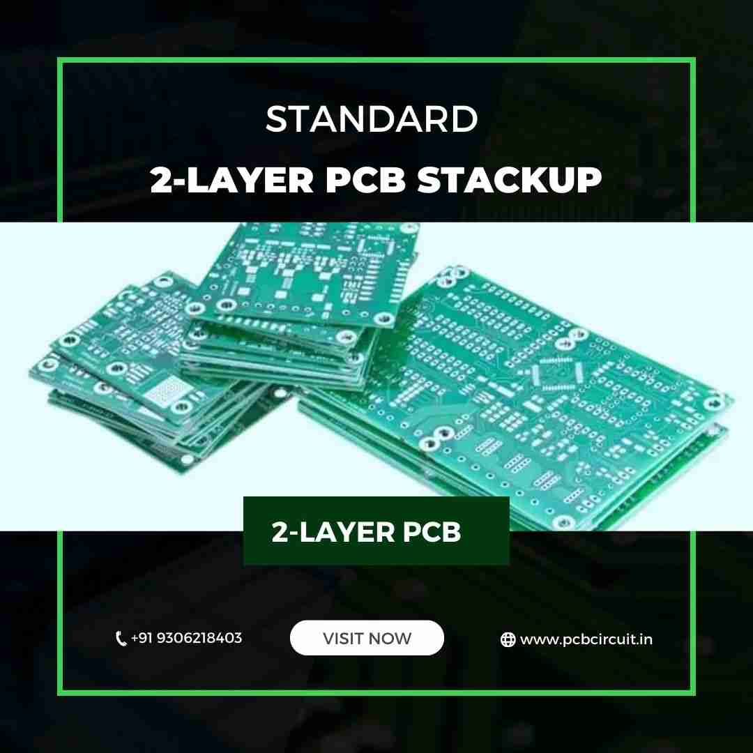
A Standard Two-layer PCB stencil typically consists of a top layer for component placement, a bottom layer for routing traces, and a core layer in between for signal transmission. This configuration offers balanced impedance control, ease of manufacturing, and cost-effectiveness for a wide range of electronic applications.
Visit us: https://bit.ly/3S4XGZm
Like


Comment
Share